Laser Cutting and Drilling
Laser Cutting and Drilling of Carbon Fiber Reinforced Polymer
Cutting and Drilling Flex PCBs
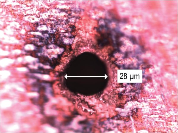
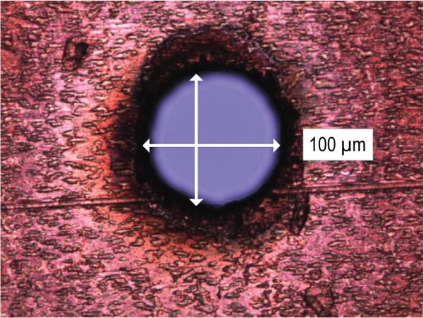
The trend in flexible PCB technology is towards miniaturization: thinner substrate materials and smaller hole sizes for both blind via holes and through vias, with concurrent increases in feature density. These small dimensions cannot be achieved using mechanical methods or longer-wavelength lasers. UV wavelengths allow focusing the beam to a spot size sufficiently small for drilling the required hole dimensions—on the order of ø100 µm down to a few tens of microns in diameter. Figure 1 show holes drilled in a Flex PCB panel, comprised of a 25 µm-thick polyimide (PI) layer sandwiched between two 12 µm-thick copper (Cu) layers, using a Spectra-Physics Talon® 355-15 laser. Both ø30-µm blind vias (Figure 1a) and ø100-µm through-vias (Figure 1b) were drilled. Such vias can be drilled at very high speeds—limited not by the laser, but rather by the speed and accuracy of the galvanometer-based scanner.
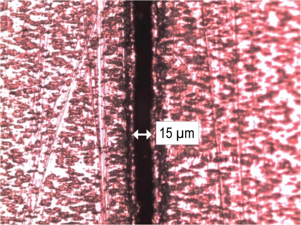
Besides drilling, laser cutting is also used in flex PCB manufacturing. Whether it be straight-line singulation or contoured profile cutting, high-speed cutting with good quality is required. The Talon UV laser was also tested for this process, with an optimized parameter set yielding a cutting speed of 215 mm/sec (see Figure 2). This was achieved with a 15 μm kerf width, and microscope inspection indicates good quality, with minimal oxidation or other heat affected zone in the copper.
Cutting Rigid FR4 PCB Panels
Another important manufacturing process that can be addressed using UV lasers is cutting of thicker, rigid PCB panels composed of fiberglass-based polymer composites such as FR4. Cutting may be necessary for depaneling (singulation) of finished devices from the larger PCB panel or for making contoured profile cuts. Figure 3 shows a 0.445 mm thick piece of FR4 cut into a 10 mm square using a 15 W Talon laser
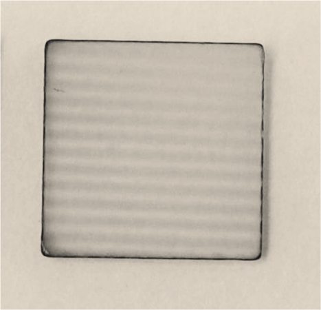
The laser’s relatively shorter-ns pulse width and variable pulse frequency allows for controlled heat input into the material. Also, with careful process optimization, the formation of carbon debris has been minimized. As with many applications, there is a tradeoff between throughput and quality. For best throughput, continuous rapid scanning cuts through the material are performed in few seconds, but with slightly higher carbonization. On the other hand, for best. quality cuts, the process is slowed down by introducing cooling delays between scans, which yields reduced throughput and much lower carbonization. The piece shown was cut at a net speed of 7.5 mm/sec.
Lithium Ion Battery Foil Cutting
Lasers for Cutting and Drilling
| Description | Features | |||
|---|---|---|---|---|
 | Spirit® High-Power Femtosecond Lasers |
| | |
 | IceFyre® UV, Green, and IR Picosecond Lasers |
| | |
 | Quasar® High Power Hybrid Fiber Lasers |
| | |
 | Talon® Diode-Pumped Solid State Q-Switched Lasers |
| |