Laser Scribing
- Ability to cleanly scribe hard or brittle materials
- Non-contact process with a low cost of operation
- Reduced chipping, micro-cracking, and de-lamination
- Narrow cut widths enable more parts per wafer
- Wider process tolerance means more robust, reliable manufacturing at a lower cost
Solar PV PERC Laser Scribing
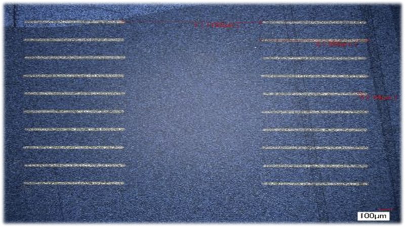
There are several key steps for fabrication PERC solar cells. First, the back side of the cell is coated with a special dielectric layer, typically SiO2 , Al2O3 , SiNx , or some combination thereof. The dielectric coating as applied is continuous, and it is therefore necessary to create openings in a subsequent process step for ohmic contact. The best way of doing this is to use a laser to ablate the dielectric film and expose the underlying silicon in the desired pattern—typically narrow linear stripes. The aluminum metallization is then applied on top of the dielectric layer. Aluminum paste is screen printed to this surface and a subsequent thermal annealing process alloys the aluminum with the laser-exposed silicon to form a good ohmic contact.
While PERC scribe geometries are somewhat varied, a 6” cell will typically have between 75 and 300 laser-scribed lines which are ~155 mm long, 30-80 µm wide, and evenly spaced by 0.5-2 mm. For the case of 1-mm line separation, the aggregate length of the PERC scribes on a single wafer is approximately 25 meters. Target processing rates demanded by industry can be as high as 3,600 WPH (wafers per hour), equating to a required scribing speed of 25 m/s. Fast 2-axis galvo scanners as well as spinning polygon scanners can achieve such speeds.
LED Scribing
Laser scribing LED wafers is a challenge since the material is relatively transparent through the visible portion of the electromagnetic spectrum. GaN is transparent below 365 nm, and sapphire is semi-transparent above 177 nm. Thus frequency tripled (355 nm) and frequency quadrupled (266 nm) diode-pumped solid state (DPSS) Q-switched lasers are the best choice for LED scribing. While excimer lasers are also available in this wavelength range, DPSS lasers have much smaller footprint and can achieve much narrower cut widths and require far less maintenance.
By reducing micro-cracking and crack propagation, laser scribing allows the LED devices to be much more closely spaced, improving both yield and throughput. Because there might typically be more than 20,000 discrete LED devices on a single 2-inch wafer, cut width critically impacts yield. Reducing micro-cracking during the die separation process has also been shown to improve the long term reliability of the LED devices. Yield is improved with laser scribing by reducing wafer breakage. The speed of the laser scribe and break process is also much faster than traditional mechanical cutting. The wider process tolerance of lasers and the elimination of blade wear and breakage translate to a more robust highly reliable manufacturing process at a lower cost.
Lasers for Scribing
| Description | Features | |||
|---|---|---|---|---|
 | Quasar® High Power Hybrid Fiber Lasers |
| | |
 | Talon® Diode-Pumped Solid State Q-Switched Lasers |
| | |
 | Explorer® One™ Compact UV and Green Lasers |
| | |
 | IceFyre® UV, Green, and IR Picosecond Lasers |
| | |
 | Millennia® eV™ High Power CW DPSS Lasers |
| |
Application Notes
LED Scribing
Amorphous Silicon Thin Film Solar Cell Scribing
Ceramic Scribing
Ceramic materials are used extensively in the microelectronics, semiconductor, and LED lighting industries because of their electrically insulating and thermally conductive properties, as well as for their hightemperature-service capabilities. Their brittleness makes laser processing attractive when compared with conventional machining, particularly for producing the increasingly small and intricate features required for advanced microelectronics packaging. See Ceramic Scribing Using Talon® Pulsed UV and Green Lasers for additional information.
Silicon Wafer Scribing
To show the advantage of TimeShift technology’s pulse splitting capability, we generated laser scribes at same scribe speed and PRF for various fluence levels. Two sets of data were collected; one with a pulse output of a single 25 ns pulse, and one with a burst of five 5 ns sub-pulses separated by 10 ns. Scribe depth data shows the clear advantage of using pulse splitting burst micromachining over single pulse machining. An increase in ablation depth between 52% and 77% was observed depending on the fluence level. We also observed improvement in quality of split pulse scribe. See Glass Cutting and Silicon Scribing Excel with Quasar® TimeShift™ Technology for additional information.