Solar / Photovoltaic Manufacturing
Driving Volume PV Production
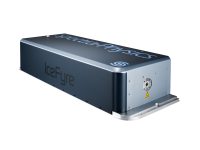
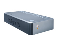
Spectra-Physics is a market leader in lasers for photovoltaic (PV) manufacturing. With thousands of lasers used in PV manufacturing, Spectra-Physics lasers deliver highest reliability and cost-effectiveness for demanding 24/7 operations. Our broad portfolio of lasers for PV is used in a variety of processes for crystalline, multi-crystalline and thin-film a-Si, CdTe and CIGS PV. Our lasers are backed by our team of applications engineers and a global support organization.
- Proven with largest installed base in PV
- Delivering disruptive cost-performance
- Powering multi-year continuous production with highest reliability
- Extensive PV applications expertise
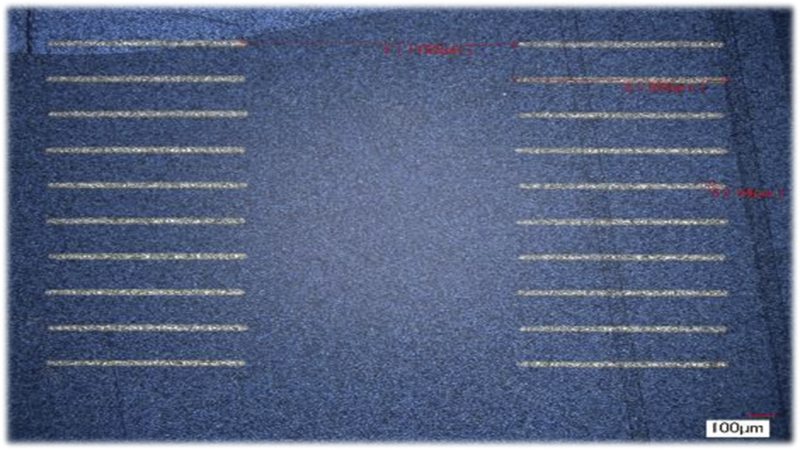
Solar PV PERC Processing
Lasers are used for creating openings in the dielectric passivation layer for ohmic contact. Aluminum paste is screen printed to this surface and a subsequent thermal annealing process alloys the aluminum with the laser-exposed silicon to form a good ohmic contact. A typical 6 inch PERC cell will have about 155 laser-scribed lines which are longer than 156 mm, 40-50 µm wide, and are separated by 1 mm. The aggregate length of the PERC scribes on a single wafer is approximately 25 m. The target processing time can be as fast as one second per wafer, which equates to a 25 m/s required scribing speed. Fast two-axis galvo scanners as well as spinning polygon scanners can achieve such speeds. Please see Newport.com for additional information on Solar Panel Manufacturing.